What Are the Key Steps in the PCB Assembly Process?
In today’s tech-driven world, understanding the PCB assembly process is crucial for anyone involved in electronics. We’ll break down the key steps to help you grasp how these essential components come to life.
Whether you’re an engineer, a hobbyist, or just curious, knowing these steps can enhance your appreciation of the technology around us. OurPCB Tech. Ltd. specializes in delivering high-quality PCB assembly services, ensuring reliability and precision in every circuit board they produce.
Understanding PCB Assembly
What Is PCB Assembly?
PCB assembly involves populating a printed circuit board (PCB) with electronic components to create functioning circuits. This critical process includes several steps, such as solder paste application, component placement, soldering, inspection, and testing. Each step ensures that the PCB performs reliably in electronic devices.
The Importance of PCB in Electronics
PCBs form the backbone of most electronic devices. They connect and support electronic components, allowing for reliable and compact designs. Without PCBs, creating efficient and scalable electronic systems would be challenging. Understanding PCB assembly helps us appreciate the complexity and precision required in modern electronics.
Pre-Assembly Steps
Design and Prototyping
In PCB assembly, design and prototyping are fundamental. Engineers begin by using software tools to create detailed schematics and layouts of the PCB. These designs outline the placement of components and trace routes. The next step involves creating a prototype to test the design’s functionality. Rapid prototyping tools help fabricate this initial model quickly, allowing for necessary adjustments before full-scale production. Testing the prototype identifies any design flaws, ensuring a reliable final product.
Sourcing Components
Sourcing components involves procuring all necessary parts for the PCB. We collaborate with trusted suppliers to acquire components such as resistors, capacitors, and integrated circuits. Quality and compatibility are crucial, so selecting reputable vendors minimizes the risk of defects. We also consider lead times and costs to maintain the project’s budget and schedule. Using reliable electronic component databases streamlines this process, ensuring all parts meet the required specifications and standards.
Main Steps in PCB Assembly
Applying Solder Paste
Applying solder paste is the first step in the PCB assembly process. We use a stencil to accurately deposit solder paste onto the PCB pads. The stencil corresponds with the PCB design, ensuring precise application. Solder paste consists of tiny particles of solder suspended in flux. It helps temporarily hold components in place and facilitates electrical connections during the soldering process.
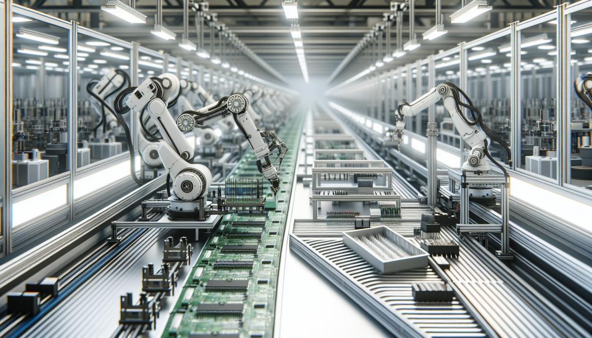
Pick and Place Machine Setup
Pick and place machines are essential for component placement. We program these machines based on the PCB layout files. The machine identifies the exact locations for components like resistors, capacitors, and integrated circuits. Using precision nozzles, it picks up each component and places it on its designated spot on the PCB. This automation increases accuracy and efficiency, reducing the risk of human error.
Soldering Techniques
Soldering secures components to the PCB. We typically use two main soldering techniques: reflow soldering and wave soldering.
- Reflow Soldering: After components are placed, the PCB passes through a reflow oven. The oven heats the solder paste, melting it to form solder joints. The PCB then cools down, solidifying the connections.
- Wave Soldering: Used for through-hole components, wave soldering involves passing the PCB over a molten wave of solder. This method ensures solder spreads uniformly, creating reliable joints.
Inspection and Quality Control
Inspection and quality control are vital steps in the PCB assembly process.
Visual Inspection
Inspectors examine the PCB visually to identify obvious defects. They look for issues like solder bridging, component misalignment, and missing components. Skilled technicians use magnification tools to enhance visibility and accuracy. This step helps catch problems early, reducing potential downstream failures.
Automated Optical Inspection (AOI)
AOI systems use cameras to scan the PCB for anomalies. These systems compare the board to a predefined model to detect issues such as solder deficiencies and component placement errors. AOI offers high-speed and high-accuracy inspection, ensuring consistent quality. Error data from AOI is often used to refine manufacturing processes and improve overall product reliability.
Testing and Functionality Checks
After assembling the components, testing and functionality checks ensure that PCBs work as intended.
In-Circuit Testing
In-circuit testing (ICT) targets individual components on the PCB. ICT identifies issues like open circuits, shorts, and incorrect values. We achieve this by using test probes to apply electrical signals to specific points on the PCB. Automated test equipment (ATE) controls these probes, enhancing efficiency and accuracy. Engineers rely on ICT to quickly pinpoint manufacturing defects and component failures.
Functional Testing
Functional testing validates the PCB’s overall operation within its intended application. This test replicates the real-world scenario where the PCB operates, checking for correct functionality under various conditions. Functional testing involves applying power and providing input signals to simulate actual usage. Testing software automates many of these procedures. By verifying the PCB’s performance, functional testing ensures the product meets design specifications and reliability standards.
By performing these tests, we ensure the final product’s quality and functionality, minimizing the risk of defective units reaching end-users.
Conclusion
Understanding the PCB assembly process is crucial for producing reliable electronic devices. From initial design and prototyping to the final testing stages each step ensures that our products meet high standards of quality and functionality. By leveraging advanced techniques and tools we can minimize defects and deliver superior performance. Staying informed about these key steps allows us to innovate and maintain a competitive edge in the tech industry. Let’s continue to prioritize precision and quality in our PCB assembly processes to achieve the best possible outcomes for our projects.
Frequently Asked Questions
What is PCB assembly?
PCB assembly is the process of mounting electronic components onto a printed circuit board (PCB). This involves steps such as solder paste application, component placement, and soldering to ensure all components are correctly attached and functional.
Why is solder paste application important?
Solder paste application is crucial as it provides a medium to connect the components to the PCB. Applied using a stencil, it ensures precise placement and strong electrical connections, leading to reliable and functional electronic devices.
How are components placed on a PCB?
Components are placed on a PCB using pick and place machines, which accurately position electronic parts onto the board after the solder paste has been applied. These machines enhance precision and efficiency in the assembly process.
What is the role of reflow soldering?
Reflow soldering is a technique used to melt the solder paste after the components have been placed on the PCB. The process ensures proper bonding between the components and the board, solidifying the connections after cooling down.
What is the importance of design and prototyping in PCB assembly?
Design and prototyping are critical in PCB assembly as they allow for the creation and testing of initial PCB layouts. Using software tools, engineers can refine designs, ensuring the final product meets specifications before mass production.
How does Automated Optical Inspection (AOI) work?
Automated Optical Inspection (AOI) uses cameras to scan the PCB for defects. It automatically compares the board to a predefined standard, identifying issues such as misalignments, soldering faults, or missing components.
What are the benefits of In-Circuit Testing (ICT)?
In-Circuit Testing (ICT) checks individual components on the PCB for correct placement and functionality. It ensures each part operates as intended, preventing faulty components from compromising the overall performance of the device.
Why is Functional Testing required post-assembly?
Functional Testing validates the operational performance of the assembled PCB within its intended application. It ensures the complete product functions correctly, detecting any issues that might not be apparent through individual component testing.
How does quality control improve PCB assembly?
Quality control, including visual inspection and automated systems like AOI, helps detect and address defects early in the assembly process. This step is crucial in ensuring the end product meets quality and functionality standards.
What should be considered in component sourcing for PCB assembly?
Component sourcing should prioritize quality and reliability. Collaborating with trusted suppliers and verifying component specifications ensures that the parts used in PCB assembly meet necessary standards, reducing the risk of defects and failures.


